IC Packaging & Assembly Services
From single-die wire bond to advanced 2.5D/3D heterogeneous integration. Every package type backed by in-house process engineering and JEDEC-standard qualification.
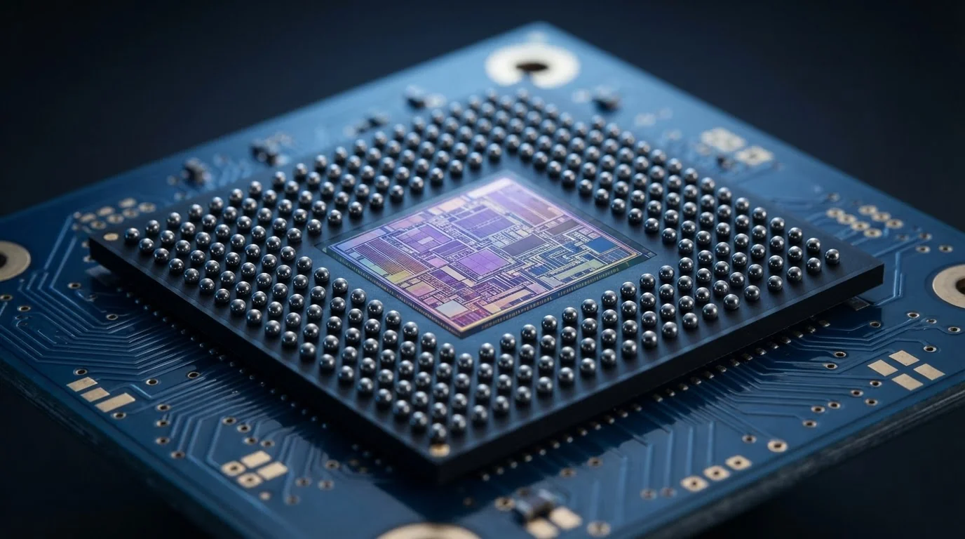
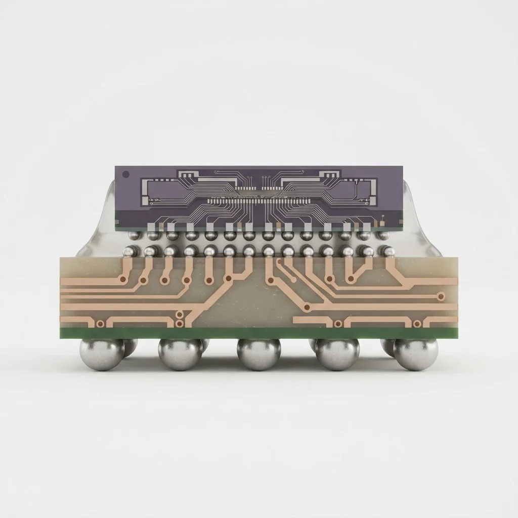
Flip Chip BGA
Controlled collapse chip connection with underfill. Fine-pitch Cu pillar and solder bump technologies for high-density interconnect.
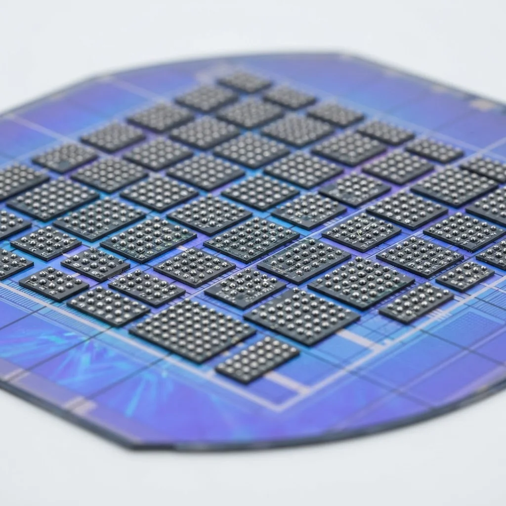
Wafer-Level CSP
Fan-in and fan-out wafer-level chip scale packaging. Redistribution layer (RDL) technology for the smallest possible footprint.
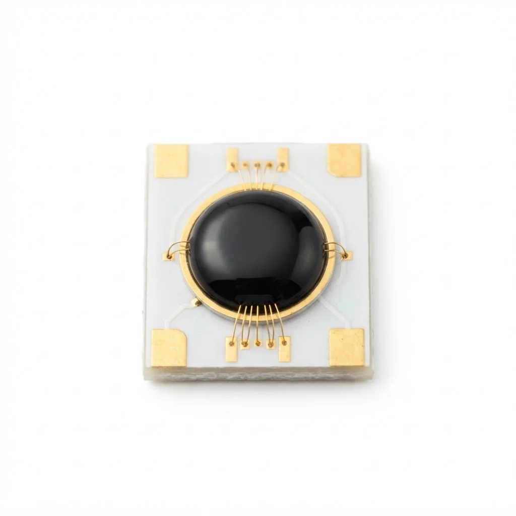
COB / COF
Chip-on-board and chip-on-flex assembly. Direct die attach with wire bonding. Black epoxy glob-top encapsulation for cost-sensitive applications.
SIP Module
System-in-package integration. Multi-die, passive component embedding, and shielded module assembly for RF, IoT, and wearable applications.
POP Stacking
Package-on-package stacking for memory-on-logic configurations. Precision placement with controlled standoff height and warpage management.
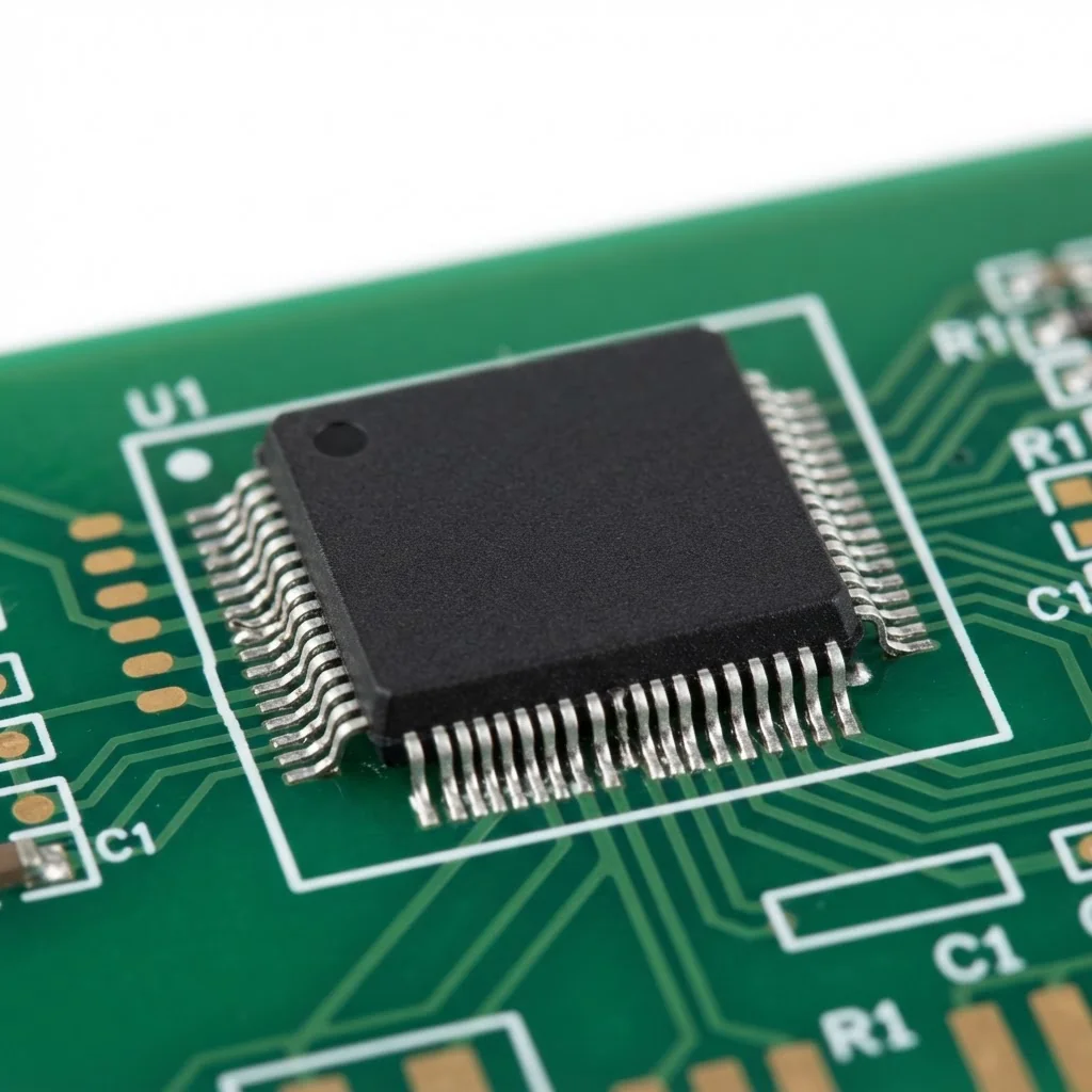
BGA / QFN / QFP
Full range of mainstream package types. PBGA, CBGA, TBGA, QFN (punched/sawn), LQFP/TQFP. Standard and custom leadframe options.
MEMS Packaging
Micro-electromechanical systems packaging with cavity and open-cavity solutions. Hermetic sealing, getter integration, and stress-isolation mounting.
Testing & Burn-In
Wafer probe, final test, system-level test, and HTOL burn-in. Custom load boards, test program development, and full ATE capability.
Technical Specifications
Our Shenzhen facility operates at the frontier of assembly capability. Every parameter verified through statistical process control.
Process Window
| Parameter | Capability | Standard |
|---|---|---|
| Max Package Body Size | 55 x 55 mm | JEDEC MO-xxx |
| Min BGA Ball Pitch | 0.3 mm | IPC-7095 |
| Max Ball Count | 2,500+ | Depopulated array |
| Wire Bond Pitch | 35 µm | Au/Cu/PdCu wire |
| Flip Chip Bump Pitch | 130 µm | Cu pillar + SAC cap |
| Die Thickness (min) | 50 µm | DBG process |
| Substrate Layer Count | Up to 14L | BT / ABF / MCE |
| Underfill Gap | 15 µm | Capillary / NCF |
| MSL Rating | Level 1-6 | J-STD-020 |
| Test Temperature Range | -55 to +175 °C | JESD22-A104 |
Ready to Package Your Silicon
Send your package drawing or requirements. Our applications engineering team responds with a technical proposal within 24 hours — including process flow, timeline, and NRE estimate.